| –≠–ª–µ–∫—Ç—Ä–æ–Ω–Ω—ã–π –∫–æ–º–ø–æ–Ω–µ–Ω—Ç: AKD4393 | –°–∫–∞—á–∞—Ç—å:  PDF PDF  ZIP ZIP |

ASAHI KASEI
[AKD4393]
<KM058804>
1
2000/5
General Description
The AKD4393 is an evaluation board for AK4393, which is 96kHz sampling 24Bit
DAC. The AKD4393
includes a LPF which can add differential analog outputs from the AK4393 and also has a digital interface with
AKM's wave generator using ROM data and AKM's ADC evaluation boards. Therefore, it is easy to evaluate the
AK4393.
<
Ordering Guide
AKD4393 Rev.C
--- Evaluation board Rev.C for AK4393: differential output
Function
<
On-board differential output buffer circuit
<
On-board clock generator
<
BNC connector for an external clock input
<
Compatible with 3types of interface
1.
Direct interface with evaluation boards for AKM's A/D converter (AKD539X, AKD535X)
2.
Interface with a signal generator (AKD43XX)
3.
On-board CS8414 as DIR which accepts optical input.
10pin Header
E x ternal
C lo c k
R O M D a ta
o r
A /D in p u t
O p tical
In p u t
C S 8414
(DIR )
C lo c k
G e n e rato r
A K 4393
2nd Order LPF
R c h
L c h
Fig.1 Block diagram
* Circuit diagram and PCB layout are attached at the end of this manual.
Evaluation board Rev.C for AK4393
AKD4393
ASAHI KASEI
[AKD4393]
<KM058804>
2
2000/5
<
External Analog Circuit (Rev.C)
The differential output circuit and LPF is implemented on board. The differential outputs of AK4393 is buffered by non-inverted
circuit and output via Cannon connector(differential output). LPF adds differential outputs. NJM5534D is used for op-amp on this
board that has low noise and high voltage torelance characteristics. Analog signal is output via Cannon and BNC connectors on the
board. The output level is about 2.94Vrms(typ@VREF=5.0V) by Cannon and 2Vrms(typ@VREF=5.0V) by BNC.
Fig.2 External Analog Filter
<
Operation sequence
1.Set up the jumpers for power supply.
[JP15(REG)] selects power supply for AVDD pin of AK4393.
short:
5V is supplied from regulator. (default)
Nothing should be connected to A5V jack.
open:
5V is supplied from A5V.
2.Set up the power supply lines.
+15V=15V, -15V=-15V:
Power supply for op-amp. AVDD of AK4393 is supplied from "+15V" through
regulator (JP15: short).
A5V=5V:
This jack is used when AVDD of AK4393 is supplied from this. In this case, JP15
should be open.
DVDD=5V:
Power supply for logic circuit on this board.
VP=3V
5.25V:
Digital (set JP10 to VP),
AGND=DGND=0V .
Each supply line should be distributed from the power unit.
3.Set up the evaluation modes by jumper pins and DIP switches.(See next item.)
4.Power on.(The AK4393 should be reset once by bringing PD "L" upon power-up.)
*SW1 resets the AK4393 during operation.
The AK4393 is reset at SW1="L" and exits resetting at SW1="H".
300
47u
300
AOUTL-
560
10n
300
220
10n
6
4
3
2
7
10u
0.1u
0.1u
10u
10u
NJM5534D
300
47u
300
AOUTL+
560
10n
300
220
10n
6
4
3
2
7
10u
0.1u
0.1u
10u
NJM5534D
3
2
1
100
100
0.1u
+
NJM5534D
0.1u
10u
100
4
3
2
4.7n
620
620
430
7
+
+
+
+
-
+
-
+
+
+
-
+
+
4.7n
Lch
-15
+15
6
430

ASAHI KASEI
[AKD4393]
<KM058804>
3
2000/5
<
The evaluation modes and corresponding jumper pins setting
1.
Evaluation Modes
∑
Applicable Evaluation Mode
(1) DIR(Optical Link)
(2) Ideal sine wave generated by ROM data
(3) Using AD converted data
(4)All interface signals including master clock are fed externally.
(1) DIR(Optical Link) (default)
PORT2 is used for the evaluation using such as CD test disk. The DIR generates MCLK, BICK and LRCK SDATAfrom
the received data through optical connector(PORT2: TORX176).
Fig.3 Jumper set-up (DIR)
(2) Ideal sine wave generated by ROM data
Digital signal generated by AKD43XX are used. PORT1 is used for the interface with AKD43XX. Master clock is sent
from AKD4393 to AKD43XX then LRCK, BICK and SDATA are sent from AKD43XX to AKD4393.
JP7
S D
JP6
L R
X T L /E X T
D IR
JP5
B I
X T L /E X T
DIR
C L K
JP9
DIR
E X T
XTL
JP8
C K D IV 1
2X
1X
JP4
B C P
INV
THR
JP2
C S 8414
V D D
GND
JP1
JP14
C K D IV 2
1/2X
1X
XTL
Fig.4 Jumper set-up (ROM data)
JP7
SD
JP6
LR
XTL/EXT
DIR
JP5
BI
XTL/EXT
DIR
CLK
JP9
DIR
EXT
XTL
JP4
JP8
CKDIV1
2X
1X
BCP
INV
THR
BCP
INV
THR
(others)
(MSB
justified)
JP2
CS8414
VDD
GND
JP1
JP14
CKDIV2
1/2X
1X
XTL
ASAHI KASEI
[AKD4393]
<KM058804>
4
2000/5
(3)
Using AD converted data
AD converted data from AKM's AD evaluation boards(AKD539X, AKD535X) is used through PORT1.
* In case of using external clock through a BNC connector, select EXT of JP9 and short JP1.
* In case of using the double speed sampling mode, select 1/2X of JP8 and set S2-2(DFS) on.
JP7
S D
JP6
L R
X T L /E X T
D IR
JP5
B I
X T L /E X T
DIR
C L K
JP9
DIR
E X T
XTL
JP8
C K D IV 1
2X
1X
JP4
B C P
INV
THR
JP2
C S 8414
V D D
GND
JP1
JP14
C K D IV 2
1/2X
1X
XTL
Fig.5 Jumper set-up (A/D)
(3) All interface signals including master clock are fed externally.
Under the following set-up, MCLK, LRCK and SCLK signals needed for the D/A to operate could be fed through PORT1.
JP7
S D
JP6
L R
X T L /E X T
D IR
JP5
B I
X T L /E X T
DIR
C L K
JP9
DIR
E X T
XTL
JP8
C K D IV 1
2X
1X
JP4
B C P
INV
THR
JP2
C S 8414
V D D
GND
JP1
JP14
C K D IV 2
1/2X
1X
XTL
Fig.6 Jumper set-up (ext.)
2. MCLK
set-up
When the LRCK is fed from the 74HC4040 on the board, The ratio of MCLK to LRCK can be selected by JP8 and JP14.
JP14
JP8
X'tal
MCLK
fs
MCLK/LRCK
1X
1X
12.288MHz
12.288MHz
48kHz
256
1X
2X
24.576MHz
24.576MHz
48kHz
512
1/2X
1X
24.576MHz
12.288MHz
96kHz
128
1/2X
2X
49.152MHz
12.288MHz
96kHz
128
Table.1 set-up example
3. BICK
set-up
When BICK is supplied from U1(74HC4040), either 32fs or 64fs could be
selected. Fig.8 shows 64fs mode. 64fs mode is recommended.
*Only mode 0(LSB justified 16bit mode) can correspond to 32fs.
Fig.7 Jumper Set-up (BCS)
JP3
B C S
64
32
ASAHI KASEI
[AKD4393]
<KM058804>
5
2000/5
4. DIP switch set-up
Confirm the set-up of the DIP switch before the operation. "ON" means "H" and "OFF" means "L".
4-1. Set-up of SW3, SW4(Mode set-up of AK4393: see the data sheet of AK4393)
DIF2
DIF1
DIF0
Mode
BICK
OFF
OFF
OFF
0: LSB justified, 16bit
32fs
OFF
OFF
ON
1: LSB justified, 20bit
40fs
OFF
ON
OFF
2: LSB justified, 24bit
48fs
OFF
ON
ON
3: I
2
S
48fs
(default)
ON
OFF
OFF
4: MSB justified, 24bit
48fs
Table 2 Audio Serial Interface Format Select Pins (SW3-5,6,7)
4-2. Set-up of SW6 (Mode set-up of CS8414. About details, see the data-sheet of CS8414)
Adjust the audio data format of CS8414 (DIR) to AK4393. CS8414 does not match the LSB justified 20bit/24bit mode of
AK4393.
M3
(SW6-2)
M2
(SW6-3)
M1
(SW6-4)
M0
(SW6-5)
Data format
JP4
OFF
OFF
OFF
OFF
MSB justified, 24bit
INV
OFF
OFF
ON
OFF
I
2
S
THR
(default)
OFF
ON
OFF
ON
LSB justified, 16bit
THR
Table 3. Set-up of SW6
SW6-1 (SEL): Usually ON.
SW6-6 (CS12): Select the channel for indicating the channel status.
ON: Rch (default), OFF: Lch
5. Parallel/Serial Control
SW5: set up P/S pin of AK4393.
H: parallel mode. PORT3 is used JP11, 12 and 13 should be open.
L: serial mode. PORT3 is used. JP11, 12 and 13 should be open.
6. Other set-up
SW1: Reset of AK4393. Select "H" during operation.
SW2: Soft-mute of AK4393. The soft-mute is executed during SW2 pushed.
LE1 : This LED shows pre-emphasis status. It turns on when the data is pre-emphasized.
LE2 : This LED shows the output of VERF pin in CS8414. It turns on when the error is occured in CS8414.

ASAHI KASEI
[AKD4393]
<KM058804>
6
2000/5
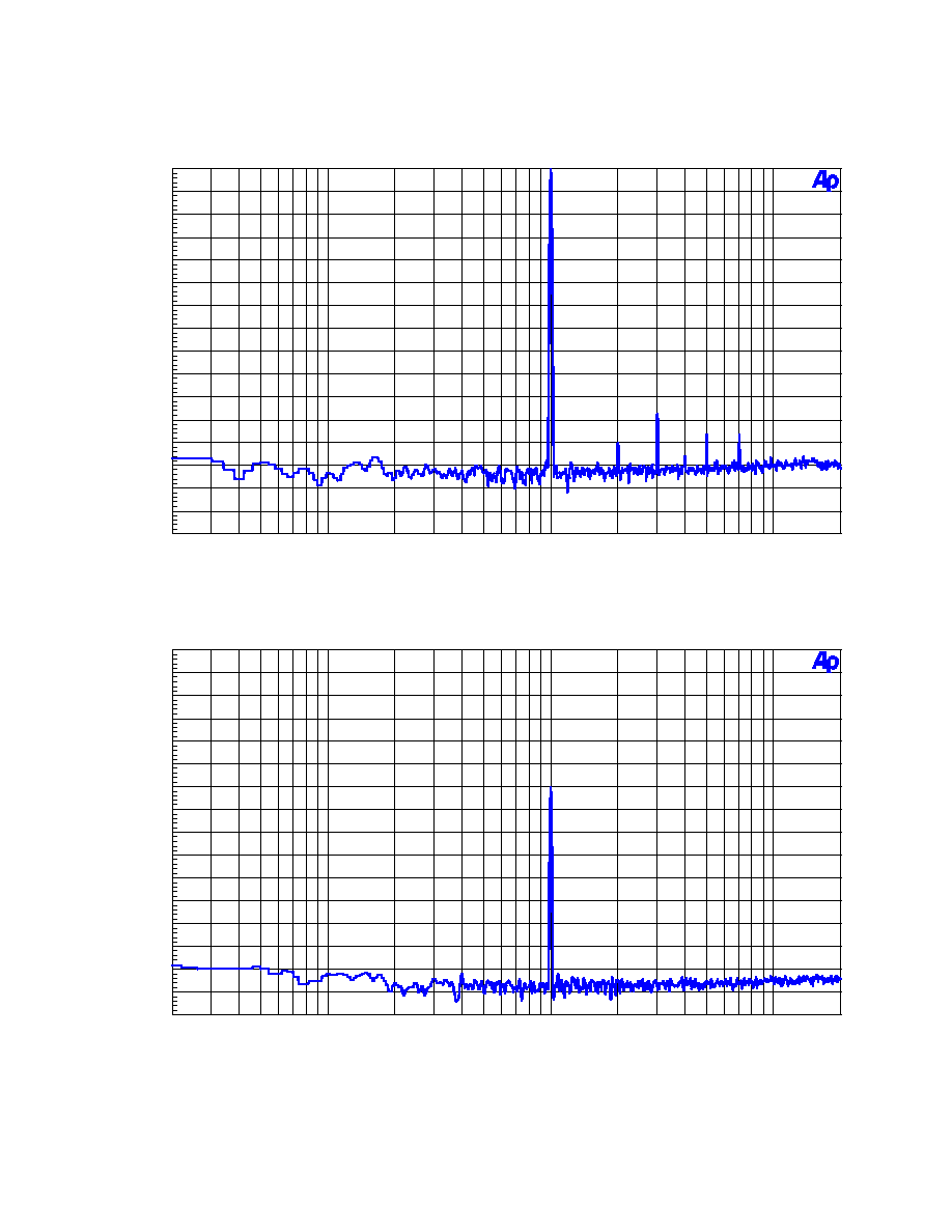
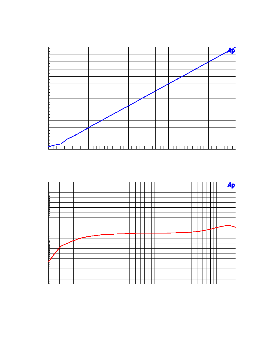
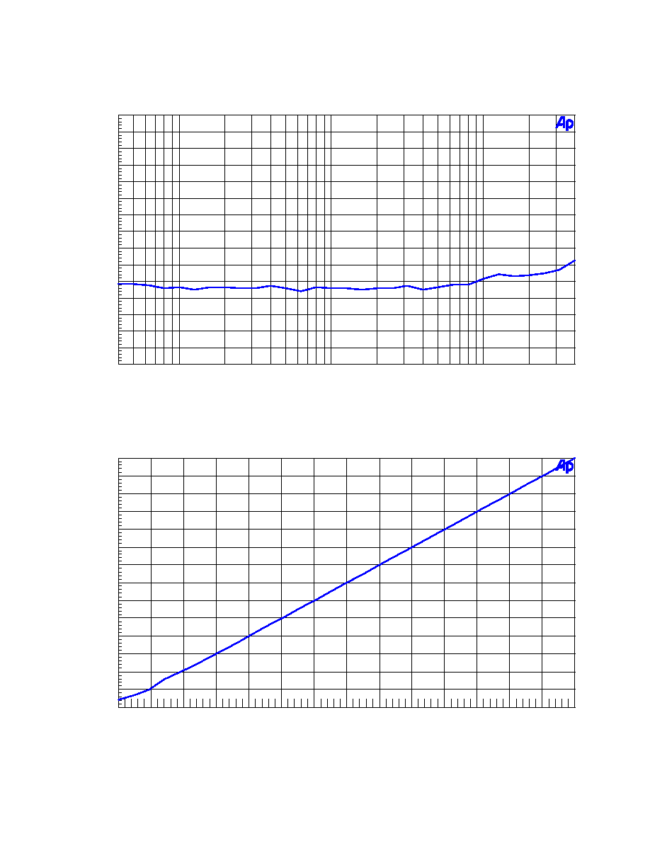
< AK4393 Measurement Example
Conditions:
AVDD =DVDD= 5.0V
Interface = DIR (44.1kHz, 96kHz)
MCLK = 256fs(fs=44.1kHz, 96kHz)
BICK = 64fs
fs = 44.1kHz, 96kHz
Input data = 24bit
Measurement unit: Audio Precision System Two Cascade (fs=44.1kHz, 96kHz)
(AKD4393 Rev.C: differential output)
fs
Result
THD+N
102.3
20kLPF
DR
120.0
22kLPF + A-weighted
44.1kHz
S/N
119.9
22kLPF + A-weighted
THD+N
100.9
40kLPF
DR
119.5
80kLPF + A-weighted
96kHz
S/N
119.7
80kLPF + A-weighted
Plot
FFT Point: 16384
Window: Equiripple
Averages: 4
ASAHI KASEI
[AKD4393]
<KM058804>
7
2000/5
(fs=44.1kHz)
A K M
A K 4 3 9 3 F F T (Input Leve=0dBFS,fin=1kHz)
-160
+ 0
-150
-140
-130
-120
-110
-100
-90
-80
-70
-60
-50
-40
-30
-20
-10
d
B
r
A
20
20k
50
100
200
500
1k
2k
5k
10k
Hz
FFT (Input Level=0dBFS, fin=1kHz)
A K M
A K 4 3 9 3 F F T (Input Leve=-60dBFS,fin=1kHz)
-160
+ 0
-150
-140
-130
-120
-110
-100
-90
-80
-70
-60
-50
-40
-30
-20
-10
d
B
r
A
20
20k
50
100
200
500
1k
2k
5k
10k
Hz
FFT (Input Level=-60dBFS, fin=1kHz)

ASAHI KASEI
[AKD4393]
<KM058804>
8
2000/5
(fs=44.1kHz)
A K M
A K 4 3 9 3 F F T (Input = "0"data)
-160
+ 0
-150
-140
-130
-120
-110
-100
-90
-80
-70
-60
-50
-40
-30
-20
-10
d
B
r
A
20
20k
50
100
200
500
1k
2k
5k
10k
Hz
FFT (noise floor)
A K M
A K 4 3 9 3 F F T (Input = "0"data,out-of band)
-160
+ 0
-150
-140
-130
-120
-110
-100
-90
-80
-70
-60
-50
-40
-30
-20
-10
d
B
r
A
90
100k
200
500
1k
2k
5k
10k
20k
50k
Hz
FFT (noise floor, out-of band)

ASAHI KASEI
[AKD4393]
<KM058804>
9
2000/5
(fs=44.1kHz)
A K M
AK4393 THD + N vs Amplitud e (fin=1kHz)
-120
-90
-118
-116
-114
-112
-110
-108
-106
-104
-102
-100
-98
-96
-94
-92
d
B
r
A
-140
+ 0
-130
-120
-110
-100
-90
-80
-70
-60
-50
-40
-30
-20
-10
d B F S
THD + N vs Amplitude (fin=1kHz)
A K M
AK4393 THD + N vs Input Frequency(Input Level=0dBFS)
-120
-90
-118
-116
-114
-112
-110
-108
-106
-104
-102
-100
-98
-96
-94
-92
d
B
r
A
20
20k
50
100
200
500
1k
2k
5k
10k
Hz
THD + N vs Input Frequency (Input Level=0dBFS)
ASAHI KASEI
[AKD4393]
<KM058804>
10
2000/5
(fs=44.1kHz)
A K M
A K 4 3 9 3 L inearity
-140
+ 0
-130
-120
-110
-100
-90
-80
-70
-60
-50
-40
-30
-20
-10
d
B
r
A
-140
+ 0
-130
-120
-110
-100
-90
-80
-70
-60
-50
-40
-30
-20
-10
d B F S
Linearity (fin=1kHz)
A K M
A K 4 3 9 3 F requency Response
-1
+ 1
-0.9
-0.8
-0.7
-0.6
-0.5
-0.4
-0.3
-0.2
-0.1
+ 0
+0.1
+0.2
+0.3
+0.4
+0.5
+0.6
+0.7
+0.8
+0.9
d
B
r
A
20
20k
50
100
200
500
1k
2k
5k
10k
Hz
Frequency Response (Input Level=0dBFS)

ASAHI KASEI
[AKD4393]
<KM058804>
11
2000/5
(fs=44.1kHz)
A K M
A K 4 3 9 3 C rosstalk
-140
-50
-135
-130
-125
-120
-115
-110
-105
-100
-95
-90
-85
-80
-75
-70
-65
-60
-55
d
B
r
A
20
20k
50
100
200
500
1k
2k
5k
10k
Hz
Crosstalk (upper = Rch, Lower = Lch)

ASAHI KASEI
[AKD4393]
<KM058804>
12
2000/5
(fs=96kHz)
A K M
A K 4 3 9 3 F F T (Input Level= 0dBFS,fin=1kHz, Notch)
-160
+ 0
-150
-140
-130
-120
-110
-100
-90
-80
-70
-60
-50
-40
-30
-20
-10
d
B
r
A
40
40k
50
100
200
500
1k
2k
5k
10k
20k
Hz
FFT (Input Level=0dBFS, fin=1kHz, notch)
A K M
A K 4 3 9 3 F F T (Input Level= -60dBFS,fin=1kHz)
-160
+ 0
-150
-140
-130
-120
-110
-100
-90
-80
-70
-60
-50
-40
-30
-20
-10
d
B
r
A
40
40k
50
100
200
500
1k
2k
5k
10k
20k
Hz
FFT (Input Level=-60dBFS, fin=1kHz)

ASAHI KASEI
[AKD4393]
<KM058804>
13
2000/5
(fs=96kHz)
A K M
A K 4 3 9 3 F F T (Input = "0"data)
-160
+ 0
-150
-140
-130
-120
-110
-100
-90
-80
-70
-60
-50
-40
-30
-20
-10
d
B
r
A
40
40k
50
100
200
500
1k
2k
5k
10k
20k
Hz
FFT (noise floor)
A K M
AK4393 THD + N vs Amplitud e (fin=1kHz)
-120
-90
-118
-116
-114
-112
-110
-108
-106
-104
-102
-100
-98
-96
-94
-92
d
B
r
A
-140
+ 0
-130
-120
-110
-100
-90
-80
-70
-60
-50
-40
-30
-20
-10
d B F S
THD + N vs Amplitude (fin=1kHz)
ASAHI KASEI
[AKD4393]
<KM058804>
14
2000/5
(fs=96kHz)
A K M
AK4393 THD + N vs Input Frequency (Input Level=0dBFS)
-110
-80
-108
-106
-104
-102
-100
-98
-96
-94
-92
-90
-88
-86
-84
-82
d
B
r
A
40
40k
50
100
200
500
1k
2k
5k
10k
20k
Hz
THD + N vs Input Frequency (Input Level=0dBFS)
A K M
A K 4 3 9 3 L inearity
-140
+ 0
-130
-120
-110
-100
-90
-80
-70
-60
-50
-40
-30
-20
-10
d
B
r
A
-140
+ 0
-130
-120
-110
-100
-90
-80
-70
-60
-50
-40
-30
-20
-10
d B F S
Linearity (fin=1kHz)

ASAHI KASEI
[AKD4393]
<KM058804>
2000/05
15
(fs=96kHz)
A K M
A K 4 3 9 3 C rosstalk
-1
+ 1
-0.9
-0.8
-0.7
-0.6
-0.5
-0.4
-0.3
-0.2
-0.1
+ 0
+0.1
+0.2
+0.3
+0.4
+0.5
+0.6
+0.7
+0.8
+0.9
d
B
r
A
40
40k
50
100
200
500
1k
2k
5k
10k
20k
Hz
Frequency Response (Input Level=0dBFS)
A K M
A K 4 3 9 3 C rosstalk
-140
-50
-135
-130
-125
-120
-115
-110
-105
-100
-95
-90
-85
-80
-75
-70
-65
-60
-55
d
B
r
A
20
20k
50
100
200
500
1k
2k
5k
10k
Hz
Crosstalk (upper = Rch, Lower = Lch)

ASAHI KASEI
[AKD4393]
<KM058804>
2000/05
16
IMPORTANT NOTICE
∑
These products and their specifications are subject to change without notice. Before
considering any use or application, consult the Asahi Kasei Microsystems Co., Ltd. (AKM)
sales office or authorized distributor concerning their current status.
∑
AKM assumes no liability for infringement of any patent, intellectual property, or other right in
the application or use of any information contained herein.
∑
Any export of these products, or devices or systems containing them, may require an export
license or other official approval under the law and regulations of the country of export
pertaining to customs and tariffs, currency exchange, or strategic materials.
∑
AKM products are neither intended nor authorized for use as critical components in any
safety, life support, or other hazard related device or system, and AKM assumes no
responsibility relating to any such use, except with the express written consent of the
Representative Director of AKM. As used here:
(a) A hazard related device or system is one designed or intended for life support or
maintenance of safety or for applications in medicine, aerospace, nuclear energy, or other
fields, in which its failure to function or perform may reasonably be expected to result in
loss of life or in significant injury or damage to person or property.
(b) A critical component is one whose failure to function or perform may reasonably be
expected to result, whether directly or indirectly, in the loss of the safety or effectiveness
of the device or system containing it, and which must therefore meet very high standards
of performance and reliability.
∑
It is the responsibility of the buyer or distributor of an AKM product who distributes, disposes
of, or otherwise places the product with a third party to notify that party in advance of the
above content and conditions, and the buyer or distributor agrees to assume any and all
responsibility and liability for and hold AKM harmless from any and all claims arising from the
use of said product in the absence of such notification.